Welcome to Electronic Materials and Nanostructures


Nanoplatelets as a Future Light Source
[10.10.2024]
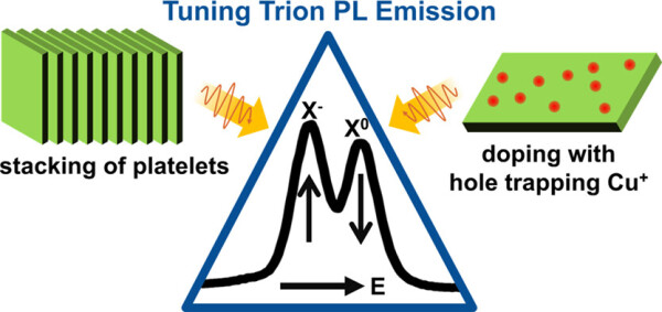
Semiconductors are fundamental materials for light-emitting diodes, solar cells, and photodetectors. By reducing the size of semiconductors to a scale of just a few nanometres, it is possible to create light sources capable of emitting single photons. Current efforts focus on integrating such light sources into various technology platforms. A promising method involves colloidal cadmium selenide (CdSe) semiconductor nanoplatelets, which are chemically synthesized in a liquid dispersion, making them easy to scale and integrate. Researchers at the Centre for Nanointegration at the University of Duisburg-Essen (CENIDE) have now demonstrated how to selectively manipulate the luminescent properties of these nanoplatelets. The journal ACS Nano reports on this.
Nanoplatelets are quasi-two-dimensional (2D) structures that are only a few atomic layers thick (approximately 1 nm) and have a lateral extent in the range of 10 to 50 nm. Due to this specific shape, they possess very defined luminescent properties, the exact origin of which has previously been unclear. Researchers from the Electronic Materials group, in collaboration with colleagues from Bilkent University in Ankara and Nanyang University in Singapore, have succeeded in elucidating the origin of this emission and developing strategies to manipulate it. A key aspect of this was the idea of isolating individual nanoplatelets and controlling the emission mechanism through targeted doping (the introduction of impurity atoms). This could represent an attractive pathway for realizing single-photon sources, which play an important role in quantum information technology.
Original publication:
M. Riesner et al., ACS Nano (2024), 18, 24523-24531
[DOI: 10.1021/acsnano.4c08776]

Job Vacancy
[08.08.2024]
Scientific Staff (f/m/d, No. 500-24)
at Chair of Electronic Materials and Nanostructures
please follow the job vacancy 500-24 (PDF file)

Graphene to increase the efficiency of UVC LEDs
[24.06.2024]
The Federal Ministry of Education and Research BMBF is funding a joint project with 2.1 million euros
The effects of the last pandemic are still being felt. Could this pandemic have been prevented or at least mitigated if suitable disinfection systems had been available? This is where AlGaN-based UVC light-emitting diodes (UVC LEDs) come into play. These emit light in the deep ultraviolet spectral range and can be used very flexibly to disinfect indoor air or surfaces thanks to their small size and long service life.
Experts agree that UVC LEDs will replace the previously used, toxic and bulky mercury vapour lamps in the future. However, commercial UVC LEDs currently still have very low efficiencies, which prevents them from being used effectively across the board. One of the main reasons for this is the very poor electrical conductivity of the so-called p-layer of the semiconductor component. A research team consisting of AIXTRON SE, Herzogenrath, as project coordinator, Protemics GMBH, Aachen, the Department of Materials in Electrical Engineering at the UDE headed by Prof Dr Gerd Bacher and ams-OSRAM International GmbH, Regensburg, as an associated partner, is pursuing a disruptive approach to solving this problem. Graphene, an atomically thin layer of carbon atoms, is to be integrated as a functional layer in UVC LEDs, thereby increasing the efficiency of UVC LEDs. The three-year joint project, funded with over 2 million euros, was preceded by a scientific BMBF preliminary project in the Department of Materials in Electrical Engineering, in which Gerd Bacher and his team were able to prove the feasibility in principle using demonstrators. Now, together with the partners, an industrial process is to be developed and scaled up to economically relevant wafer sizes. Gerd Bacher: "In the end, a technology should be available that strengthens Germany's competitiveness in the fields of electronics and optoelectronics, plant engineering and quantum technology."

Best Poster Award for M.Sc. Tamara Czerny at 10th NRW Nano Conference
[12.06.2023]
For the poster "Efficient Narrowband Photoconductivity of the Excitonic Resonance in 2D Ruddlesden-Popper Perovskites Due to Exciton Polarons" M.Sc. Tamara Czerny was awarded the Best Poster Award at the 10th NRW Nano Conference - Innovations in Materials and Applications, May 23-24, 2023 in Dortmund. The poster is about a narrow band photodetector based on a 2D perovskite thin film and the findings on the origin of charge separation, which belongs to the topic of the working group Electroenergetic Functional Materials around Jun.-Prof. Franziska Muckel.

Dr. Pradeep Kodimana Ramakrishnan receives Walter Benjamin Grant of the German Research Foundation (Deutsche Forschungsgemeinschaft):
[02.05.2023]
The German Research Foundation (DFG) awards Dr.Pradeep Kodimana Ramakrishnan,
a postdoctoral researcher working with the group of Prof. Gerd Bacher at the Werkstoffe der Elektrotechnik, University of Duisburg-Essen, the Walter Benjamin Position for the project titled: "Demystifying the Exciton-Dopant Interaction in Lead Halide Perovskites by Magneto-Optical Spectroscopy on Single Nanocrystals"
The Walter Benjamin Programme enables postdoctoral researchers at an early career phase who are associated with a German research institution or work there, to conduct independently a research project of their choice and to benefit from additional career-promoting conditions. The award finances the position for two years while the University of Duisburg-Essen covers additional project needs. The prize is named after Walter Benjamin, a German philosopher and cultural critic, who lived from 1892-1940.

Sony World Photography Awards Dr. Pradeep Kodimana Ramakrishnan received the India National Award 2023
[14.03.2023]
Aimed at supporting the best regional photographers around the globe, the Sony World Photography Awards has released its list of this year’s National winners from a record number of more than 415,000 images from more than 200 countries and territories.
The World Photography Organisation and Sony India are delighted to announce Dr. Pradeep Kodimana Ramakrishnan, a present postdoctoral researcher at the Werkstoffe der Elektrotechnik working with the group of Prof. Gerd Bacher at UDE as India’s National Award winner for the Sony World Photography Awards 2023.
The National Awards program is an initiative set up by the World Photography Organisation and Sony to support local photographic communities around the world, with 55 countries taking part this year. Over 415,000 images from over 200 countries and territories were submitted to the Sony World Photography Awards 2023 and over 200,000 were entered to the Open competition (from which the National Awards winner was selected).
Pradeep was anonymously selected by judges for his photograph Tuffie entered the Street Photography category of the Open competition. The image depicts Navigating life’s twists and turns, one step at a time. Pradeep’s photograph is stripped to the bare minimum. It focuses solely on the minimalist lines and shapes, made even more prominent by the picture's lack of colour. It was shot at the iconic location in Duisburg, the Tiger and Turtle in the last summer. He is also a member and organizer of the Düsseldorf Street Photography group. His images were published at United Nations Climate Change Conference (COP 27) 2022. He is a self-taught photographer and has learned photography through experimenting and independent study from various online sources.
As India’s National Award winner, Pradeep Kodimana Ramakrishnan receives Sony digital imaging equipment and will be included in the Sony World Photography Awards exhibition and book. All of the award-winning images will be displayed at a photography exhibition at Somerset House in London from April 14th to May 1st.

Success for the UDE DFG funds an international research training group
[09.05.2022]
Materials sciences at the UDE can further expand their research. The German Research Foundation (DFG) is funding a new International Research Training Group (IRTG) with a total of around 7.3 million euros for the first five years. The research subjects are the properties and production of two-dimensional materials.
Two-dimensional (2D) materials are extremely thin and in some cases consist of only a single layer of atoms. They are particularly interesting because they have unique electrical and optical properties and can be rolled, folded or stretched due to their high mechanical stability. The IRTG Scalable 2D Material Architectures (2D-MATURE). Synthesis and Processing, Characterization and Functionality, Implementation and Demonstration at the Faculty of Engineering with participation from the Faculty of Physics will address two questions: How can two-dimensional materials be produced in large quantities, and how do they behave when combined with other materials in ways that can be used in products?
The goal is to develop new methods and processes to enable industrial-scale applications, for example in light-emitting diodes or batteries. The IRTG is headed by Prof. Gerd Bacher (Faculty of Engineering, Department of Electrical Engineering and Information Technology). The PhD students, who are conducting research at the Center for Nanointegration Duisburg-Essen (CENIDE), will collaborate with Canadian colleagues at the Waterloo Institute of Nanotechnology (WIN) at the University of Waterloo and also spend several months there.
Dr. Thomas Wittek, press office UDE


