Integrated Photonics
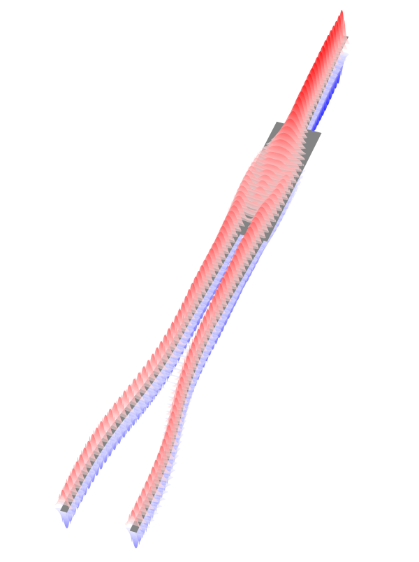
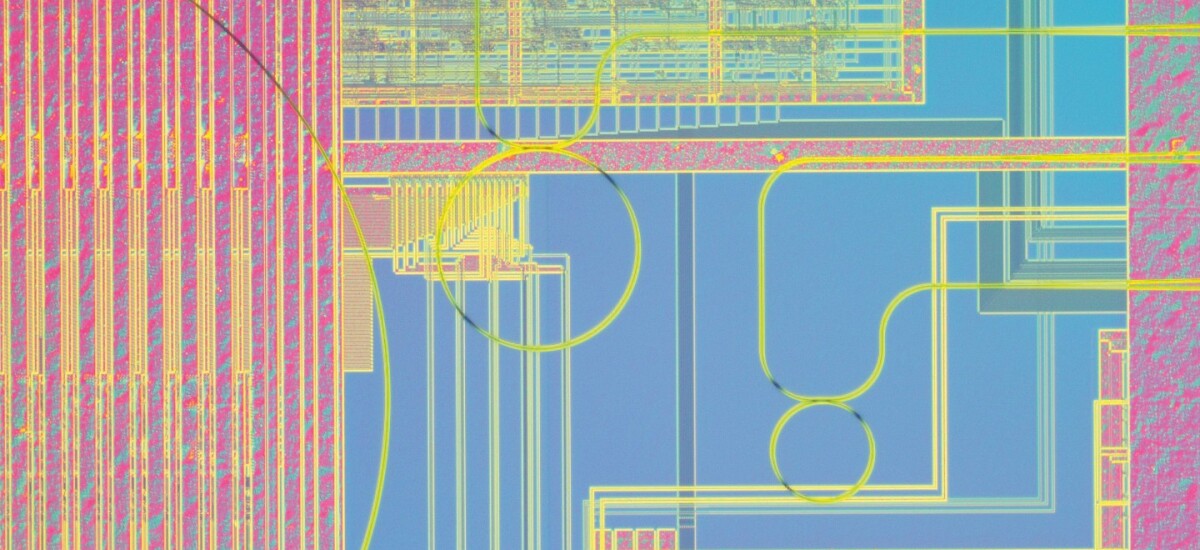
The team from the Department of Electronic Components and Circuits (EBS) at the University of Duisburg-Essen (UDE) is working together with the Fraunhofer Institute for Microelectronic Circuits and Systems (IMS) on the development of innovative photonic integrated circuits (PICs). This collaboration combines the expertise of both institutions to create cutting-edge solutions in photonics. The basic components for the circuit platform are simulated and characterised at EBS. This work forms the foundation for the integration of the technology at Fraunhofer IMS.
The research focuses on three main areas: The development of energy-efficient large-scale circuits that meet the increasing requirements for data processing and transmission and complex sensor systems. Secondly, research into non-linear materials that open up new possibilities for complex optical functions. Thirdly, the development of quantum photonic devices that have the potential to revolutionise quantum communication and information processing. We are pushing the boundaries of integrated photonics and laying the foundations for future innovations in this dynamic field of research.

Prof. Anna Lena Schall-Giesecke
Projects
Mobile Material Characterization and Localization by Electromagnetic Sensing
The vision of MARIE is to precisely and dynamically characterize and localize even moving materials in our daily surroundings. In order to achieve this vision, suitable devices and overall systems are needed to carry out the localization, characterization and visualization of materials.The final goal is the achievement of a mobile MAteRIal TranscEiver that can either be interpreted as a novel compact sensory organ that extends the human senses or, on a more industrial level, as a device that systematically creates material maps for searching and classifying objects in arbitrary environments.
Our subproject S01 combines the expertise of different research groups at the universities UDE and RUB dealing with broadband transmit beamforming and beam steering concepts, as well as the expertise of Prof. Schall-Giesecke's group in the field of photonic platforms and integration techniques. This synergy aims to develop and advance concepts for high-speed beamforming in the terahertz frequency range.
FouRiEr Domain ElectRIcal-to-optical Converter (FREDERIC)
The aim of this project is to demonstrate the functionality of a novel digital electronic-photonic transmitter concept that utilises the properties of the well-known Fourier transform. For this purpose, an FD DAC (Fourier-domain digital-to-analogue converter) is combined with a frequency comb. This combination promises a massive parallelism of the signals to be transmitted and at the same time a reduction in the demands on the electrical subsystems.
Publications in the field of integrated photonics
Westhues, M., Geruschke, T., Hauser, J., Burkard, R., Nesic, A., Schall-Giesecke, A.L. (2024). Highly Flexible Dielectric Platform for Post-CMOS Photonics. In: Witzens, J., Poon, J., Zimmermann, L., Freude, W. (eds) The 25th European Conference on Integrated Optics. ECIO 2024. Springer Proceedings in Physics, vol 402. Springer, Cham. https://doi.org/10.1007/978-3-031-63378-2_96
Schaberg, Lars Leander; Kubiczek, Tobias; Santhakumaran, Sabisan; Burkard, Roman; Mertin, Wolfgang; Muckel, Franziska; Bacher, Gerd; Schall-Giesecke, Anna Lena; Neumaier, D.; Balzer, Jan C.; Kirchner, Elsa Andrea; Benson, Niels: Body Motion detection using epidermal electronic graphene patches. (Annual Conference of the German Society for Biomedical Engineering (BMT) <57, 2023, Duisburg>). In: Biomedical Engineering = Biomedizinische Technik 68 (2023), s1, [p. 13]. DOI: 10.1515/bmte-2023-2001
Equipment at the department

Measuring setup Electro-optical characterisation of photonic structures
Measurement options:
- Side coupling of PICs
- Up to 8’ wafers with grating couplers using single fibres or fibre arrays
Devices and components:
- Tunable laser source
(wavelength range: 1510 nm - 1640 nm; optical output power up to +7 dBm) - Erbium-doped fibre amplifier
(wavelength range: 1525 nm - 1565 nm; optical output power up to +15 dBm) - Fibre-coupled detectors DC up to 22 GHz
- Laser sources in the visible range
- Various active and passive fibre components (modulators, optical switches, fibre optic couplers / splitters, fibre arrays, ...)
Measuring setup Electro-optical material characterisation
Measurement options:
- Determination of the electro-optical coefficients in the wavelength range from 1510 nm to 1640 nm
Devices and components:
- Polarimeter
- Soleil-Babinet compensator
- Lock-in amplifier
- Low-noise voltage and current amplifier
- Various optical components (wave plates, polarisation filters, apertures, ...)

Design- and Simulations-Software
- Cadence tools for the design and simulation of electrical circuits and the creation of layouts
- COMSOL for multiphysical simulation
- Ansys Lumerical for the design and simulation of photonic components and circuits
- Synopsys TCAD for process simulation and process development
Equipment at Fraunhofer IMS
The close cooperation with Fraunhofer IMS gives us access to a modern cleanroom infrastructure for the production of photonic structures on 200 mm wafers, which are manufactured using a 350 nm technology node and 248 nm DUV lithography. Processes for LPCVD and PECVD silicon nitride are available in the cleanroom, including a variant with improved properties in the visible wavelength range, allowing specific requirements to be met. ALD processes for the deposition of photonic materials such as tantalum pentoxide and sputtering systems for the deposition of aluminium nitride are also available. Planarisation options are available for the heterogeneous integration of III-V semiconductor components, for example, and the development of process sequences for the direct integration of photonic structures on electronic circuits is currently in development. This enables us to realise application-specific designs and requirements flexibly and efficiently.


