Transmission Electron Microscopy
Interdisplinary Center for Analytics at the Nanoscale (ICAN) Transmission Electron Microscopy
We offer crystallographic, chemical and morphological analysis for various materials by means of high-resolution and analytical transmission electron microscopy.

Si spheres (FIB lamella): diffraction and HRTEM
(click on the picture to enlarge)
(left) TEM image of FIB lamella sample containig cross-section of three Si spheres (1,2,3) with corresponding single-crystal diffraction patterns.
(right) TEM image of Si sphere "3" and high resolution image of the area marked with the blue square.
(Sample: courtesy of Martin Meseth, TEM measurements: Anna Elsukova)

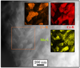
Co-Cr-Mo alloy: EDX map
(click on the picture to enlarge)
HAADF-STEM image of the Co-Cr-Mo alloy with corresponding elemental maps of characteristic x-ray Co, Cr and Mo K-lines. EDX maps were acquired from the region marked by an orange square.
(Sample: courtesy of Priska Stemmer ,TEM measurements: Anna Elsukova)

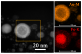
Fe@Au core shell nanoparticle: EDX map
(click on the picture to enlarge)
HAADF-STEM image of the Fe@Au nanoparticle with corresponding elemental maps of characteristic x-ray Fe K-line and Au M-line. EDX maps were acquired from the region marked by an orange square.
(Sample: courtesy of Jurij Jakobi, TEM measurements: Anna Elsukova)

