Münzer Research Group (formerly Muckel Research Group)
The development of flexible optoelectronic systems as a further development of rigid components opens up a wide range of new application possibilities, for example in medical technology, wearables or consumer electronics. The flexibility allows for integration on irregular surfaces such as clothing or directly on the skin, increasing comfort for wearable applications. They are also light and thin, ideal for devices with limited space or weight. Flexible optoelectronics can be produced efficiently through simple, cost-effective manufacturing methods, for example from the solution, which opens up new, innovative fields of application. Conventional flexible components are made of organic semiconductors, which have a high degree of mechanical flexibility, but have deficits in electrical mobility and resistance to environmental influences. The vision of the Muckel group is to replace these materials with flexible inorganic semiconductors that promise greater stability against aging processes as well as better component efficiencies due to higher electronic mobility. In particular, the group relies on 2D materials, metal-halide perovskites and colloidal nanocrystals, which it uses in light-emitting components (LEDs) and photodetectors.
The research activities can be divided into two areas:

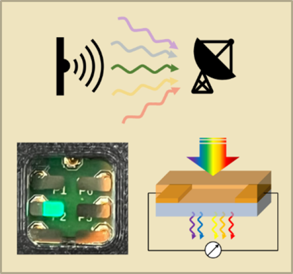
Perovskite Components for Energy-Efficient Narrowband Optoelectronic Systems
The use of specific wavelengths offers decisive advantages, especially in optoelectronic systems in which information is obtained and transferred. Since wavelength-selective systems only respond to a narrow wavelength range, it effectively minimizes interference from unwanted light and ensures higher precision and signal quality. This also allows for more energy-efficient use, as the systems can operate at lower outputs. In addition to imaging and data transmission, fields of application include optical sensor technology for medical diagnostics or machine vision for industrial automation.
A promising class of materials for the implementation of narrowband optoelectronic systems are metal-halide perovskites. These materials, which can be processed from the solution, are used as thin films in flexible components, while their optoelectronic properties can be tuned via composition. Due to their band structure with high state densities at the bandgap, perovskites exhibit very narrow emission in the range of < 30 nm, which makes them interesting for both sensor technology and colorfast displays. When voluminous ions are added, the crystal structure transforms so that two-dimensional multi-quantum layers form in a self-organized manner. These so-called 2D perovskites have high exciton exciton binding energies up to > 300 meV, which results in defined absorption resonances, which in turn are interesting for use as direct absorbers in narrowband photodetectors. The Muckel group develops narrowband LEDs and photodetectors based on the diverse possibilities of perovskite synthesis.

Flexible 2D Photodetectors for Medical Applications
Flexible sensor technology offers a wide range of advantages in medical technology in the form of portable or patient-oriented applications. Since they adapt to the contours of the body, they allow comfortable and unobtrusive monitoring of vital parameters such as heart rate, body temperature or oxygen saturation. Their flexibility and thinness make them ideal for permanent skin contact, allowing for continuous, precise measurements, especially in patients in maximum care.
2D materials consisting of only one or a few atomic or molecular layers uniquely combine a variety of properties that predestine them for use in flexible photodetectors: Thanks to their atomic thinness, they are extremely flexible and can be integrated into flexible substrates without sacrificing performance. Despite their low thickness, they offer excellent electronic mobility and are extremely sensitive to light in their conductivity. In addition, the most important 2D compounds are biocompatible. The excellent material properties are also reflected in efficient proof-of-concept components in the literature, which are mostly based on mechanically exfoliated 2D layers. In the meantime, the common semiconducting 2D materials can also be produced in scalable methods (MOCVD, CVD, chemical exfoliation). The goal of the Muckel group is to develop large-area and scalable device architectures for flexible photodetectors based on these 2D materials from industry-relevant production and by this to take the next steps towards real life applications.

